Call us (08:30-16:00 UK)
01803 865913International
+44 1803 865913Need Help?
Help pages
Wildlife Survey & Monitoring
- Aquatic Survey & Monitoring
- Professional Hand & Kick Nets
- Water Testing
- Waders & Aquatic Safety
- View All
- Amphibian & Reptile Survey
- Amphibian Survey & Monitoring
- Reptile Survey & Monitoring
- Scales, Balances & Holding Bags
- View All
Field Guides & Natural History
Academic & Professional Books
- Evolutionary Biology
- Evolution
- Human Evolution & Anthropology
- Cladistics, Phylogeny & Taxonomy
- View All
British Wildlife
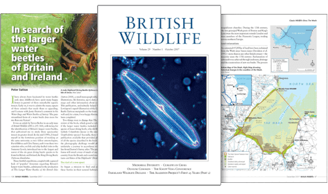
British Wildlife is the leading natural history magazine in the UK, providing essential reading for both enthusiast and professional naturalists and wildlife conservationists. Published eight times a year, British Wildlife bridges the gap between popular writing and scientific literature through a combination of long-form articles, regular columns and reports, book reviews and letters.
Conservation Land Management
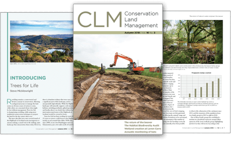
Conservation Land Management (CLM) is a quarterly magazine that is widely regarded as essential reading for all who are involved in land management for nature conservation, across the British Isles. CLM includes long-form articles, events listings, publication reviews, new product information and updates, reports of conferences and letters.