


The Travel season is an experienced travel management company. We work with you to manage all elements of your travel in an efficient, cost effective and eithical manner.
The travel season is committed to making a difference in the destination that its clients travel to, whether on business on holiday or on a study tour.
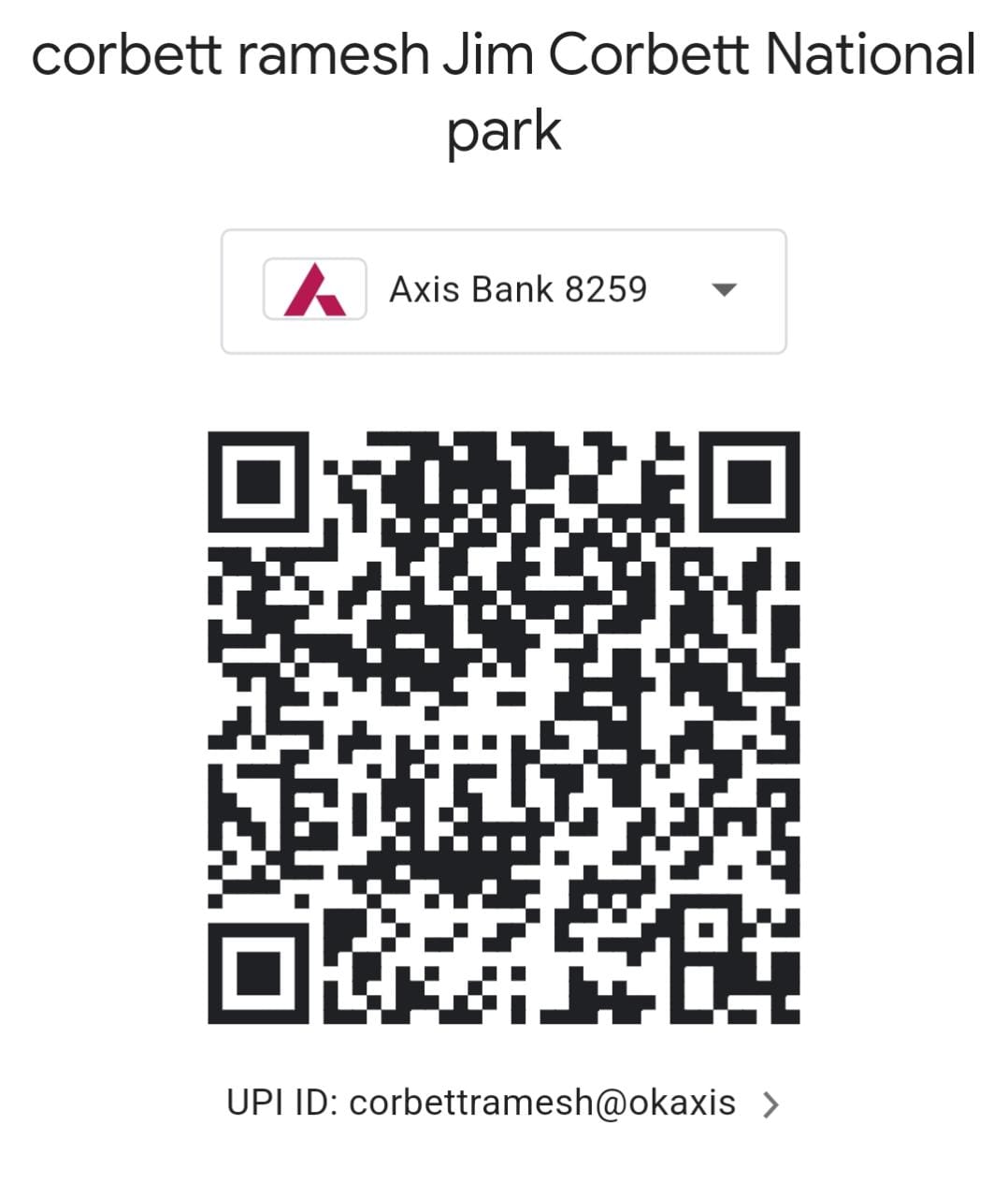
With office in Jim Corbett Uttarakhand, the company is focused on managing the travel spend up to minimum.
The UFS 3.1 pin configuration is as follows: Pin Number Pin Name Description 1-4 VCC Power supply pins 5-8 VCCQ Power supply pins 9-12 VCCQ2 Power supply pins 13-20 Data pins Data transmission pins 21-22 CLK, CLKOUT Clock pins 23-24 RESET, RESETB Reset pins 25-26 INT, INTB Interrupt pins 27-32 Reserved Reserved for future use
The Universal Flash Storage (UFS) interface has become a widely adopted standard for storage in mobile devices, laptops, and other applications. UFS 3.1 is the latest version of this interface, offering significant improvements in performance, power consumption, and capacity. In this article, we will delve into the UFS 3.1 pinout, exploring its configuration, specifications, and applications.
UFS 3.1 Pinout: A Comprehensive Guide**
In conclusion, the UFS 3.1 pinout is a critical component of the UFS 3.1 interface, providing a high-speed storage solution for a wide range of applications. Its configuration, specifications, and applications make it an ideal choice for mobile devices, laptops, gaming consoles, and automotive systems. As the demand for fast storage access and high-capacity storage continues to grow, UFS 3.1 is poised to play an increasingly important role in the storage industry.
Here is a simplified diagram of the UFS 3.1 pinout: “` +—————————————+ | UFS 3.1 | | Pinout |
Your time is important. When you choose The Travel Season, we dedicate time to organising a first-rate experience using our regional knowledge, so you can spend your own time however you please. And once you are travelling, Each day of your personalised itinerary is set up to be memorable.
Qulity, Trust, Ethical, Creativity, Efficiency. Communication. Having clearly stated and promoted values within our organisation

LOCAL SIGHT SEEN , UTTARAKHAND TOUR 24*7

LOCAL SIGHT SEEN , UTTARAKHAND TOUR 24*7

LOCAL SIGHT SEEN , UTTARAKHAND TOUR 24*7

LOCAL SIGHT SEEN , UTTARAKHAND TOUR 24*7
The UFS 3.1 pin configuration is as follows: Pin Number Pin Name Description 1-4 VCC Power supply pins 5-8 VCCQ Power supply pins 9-12 VCCQ2 Power supply pins 13-20 Data pins Data transmission pins 21-22 CLK, CLKOUT Clock pins 23-24 RESET, RESETB Reset pins 25-26 INT, INTB Interrupt pins 27-32 Reserved Reserved for future use
The Universal Flash Storage (UFS) interface has become a widely adopted standard for storage in mobile devices, laptops, and other applications. UFS 3.1 is the latest version of this interface, offering significant improvements in performance, power consumption, and capacity. In this article, we will delve into the UFS 3.1 pinout, exploring its configuration, specifications, and applications. ufs 3.1 pinout
UFS 3.1 Pinout: A Comprehensive Guide**
In conclusion, the UFS 3.1 pinout is a critical component of the UFS 3.1 interface, providing a high-speed storage solution for a wide range of applications. Its configuration, specifications, and applications make it an ideal choice for mobile devices, laptops, gaming consoles, and automotive systems. As the demand for fast storage access and high-capacity storage continues to grow, UFS 3.1 is poised to play an increasingly important role in the storage industry. The UFS 3
Here is a simplified diagram of the UFS 3.1 pinout: “` +—————————————+ | UFS 3.1 | | Pinout | Here is a simplified diagram of the UFS 3